
Application Background
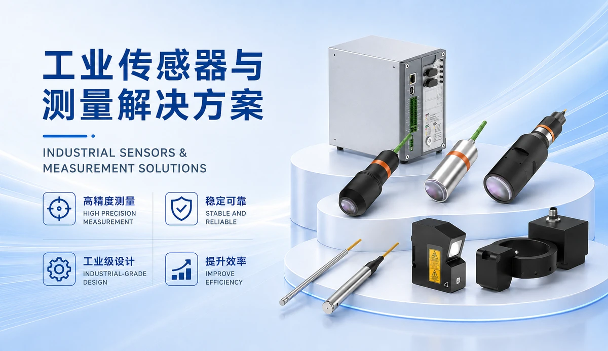
In semiconductor manufacturing and packaging, the height and positional stability of the wafer stage (vacuum chuck or carrier platform) directly affects the accuracy of wafer adsorption, handling, and processing. Stage height deviations can lead to wafer warping, fragmentation, or positioning errors, thus affecting yield. The ST-P series laser displacement sensors use laser triangulation for non-contact measurement, enabling real-time detection of stage height changes and providing closed-loop position feedback for the equipment.
Detection Objects and Purposes
Detection Objects: Surfaces of wafer chucks, vacuum stages, and carrier platforms. Detection Purposes: To determine the adsorption state (e.g., whether the wafer is completely adsorbed), stage flatness, repeatability of pick-and-place positions, and the real-time position of the Z-axis motion platform. Typical applications include wafer handling robots, probe stations, dicing machines, and pick-and-place machines.
On-site Pain Points
Wafer stage surfaces are often made of mirrored metal, ceramic, or glass, with significant differences in reflectivity, making ordinary sensors susceptible to interference.
Limited detection space necessitates compact sensors mounted on the side or below the stage.
High-speed production cycles require sensors with high sampling frequencies (e.g., above 10kHz) to capture dynamic position changes.
High environmental cleanliness is required; sensors must be dust-free or easy to clean.
Product Principle and Selection Guide
The ST-P series is based on laser triangulation. A laser beam illuminates the measured surface, and the reflected light is imaged on a CMOS/PSD image through a lens. Displacement is calculated based on position changes. Selection should be based on installation distance and accuracy requirements:
| Model | Reference Distance | Measuring Range | Repeatability | Linearity Error |
|---|---|---|---|---|
| ST-P25 | 25 mm | ±1 mm | 0.05 μm | <±0.6 μm |
| ST-P30 | 30 mm | ±5 mm | 0.15 μm | <±3 μm |
| ST-P50 | 50 mm | ±10 mm | 0.25 μm | <±4 μm |
| ST-P80 | 80 mm | ±15 mm | 0.5 μm | <±6 μm |
| ST-P150 | 150 mm | ±40 mm | 1.2 μm | <±16 μm |
For wafer stage height detection, if the installation distance is short (e.g., 25-50mm) and sub-micron accuracy is required, ST-P25 or ST-P30 are recommended; if a larger measurement range is required or installation space is limited, ST-P50 or ST-P80 can be considered. Specific selection needs to be confirmed based on the site distance, the characteristics of the measured surface, and accuracy requirements.
Solution Recommendation
Typical Solution: Install ST-P series sensors below or to the side of the stage, with the laser incident vertically or at a small angle on the stage surface. The sensors output height data to a PLC or motion controller via Ethernet or RS485 to achieve closed-loop position adjustment. For multi-station stages, multiple sensors can be configured for simultaneous measurement to evaluate flatness or warpage. The signal output supports analog signals (4-20mA/0-10V) and I/O, facilitating integration with existing systems.
Installation and Commissioning Recommendations
During installation, ensure the sensor is perpendicular to the surface being measured to avoid measurement errors caused by tilting.
For mirrored or transparent surfaces (such as polished silicon wafers), sample testing is recommended. Adjust laser power or use a diffuse reflection target if necessary.
The sensor should be securely fixed to prevent vibration from affecting repeatability.
During commissioning, calibrate the zero point first, then set the measurement range according to the actual travel.
Note the sensor's operating temperature range (must be confirmed based on the specific model) to avoid thermal drift.
Frequently Asked Questions
Q: The wafer surface has strong reflections; can the sensor provide stable measurements?
A: The ST-P series is optimized for different surface reflection characteristics, but strong specular reflection may cause signal saturation. Sample testing is recommended first; adjust the mounting angle or use a polarizer if necessary.
Q: What is the maximum sampling frequency of the sensor? Can it meet the requirements of high-speed handling?
A: The ST-P series has a maximum sampling frequency of 160kHz; specific frequencies need to be confirmed based on the model. For general wafer handling (cycle time < 1s), a frequency of 10kHz or higher is sufficient.
Q: How to connect to a PLC?
A: Supports Ethernet (Modbus TCP), RS485 (Modbus RTU), analog signals, and IO output. The appropriate PLC interface can be selected.
Summary
The ST-P series laser displacement sensors provide a high-precision, non-contact solution for wafer stage height and position detection. With proper selection and installation, the positioning accuracy and yield of semiconductor equipment can be effectively improved. In practical applications, it is recommended to conduct sample testing on specific materials (such as wafers, ceramics, glass, and encapsulating adhesives) to verify measurement stability. This article explains the selection approach; final models and parameters should be confirmed against product data and sample-test results.