Application Background
In semiconductor manufacturing and packaging, wafer surface height, flatness, and warpage directly affect process quality in lithography, etching, and thin-film deposition. Traditional contact measurement risks damaging wafers and has low efficiency, making non-contact laser displacement sensors an ideal choice. The ST-P series, based on laser triangulation, achieves micron or even sub-micron accuracy, suitable for wafer inspection, stage calibration, and handling positioning.
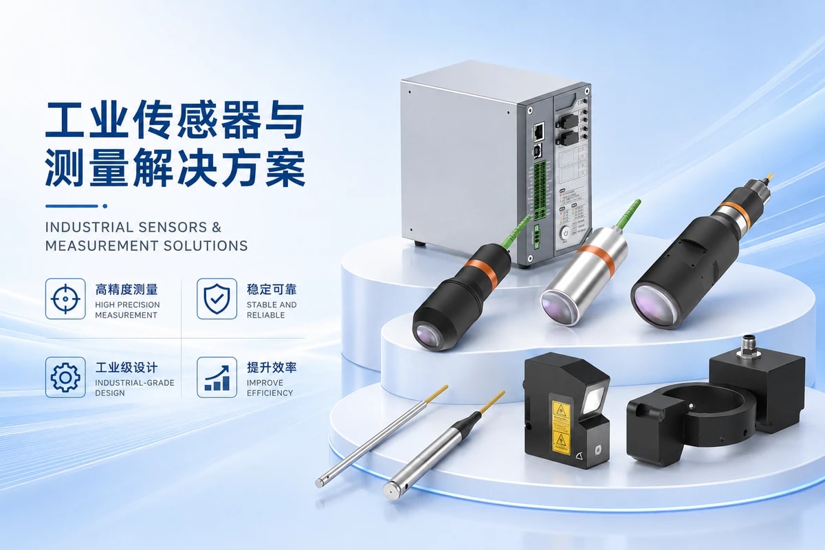
Product Principle and Selection Guide
Measurement Principle
The ST-P series uses laser triangulation: a laser beam is projected perpendicularly or at an angle onto the target surface, and the reflected light is imaged onto a CMOS/PSD detector. Displacement is calculated from the spot position change. The non-contact method avoids wafer scratches and works with mirror, transparent, or low-reflectivity materials.
Model Selection
Based on measurement distance and accuracy requirements, the ST-P series offers multiple models:
- ST-P25: Reference distance 25 mm, measurement range ±1 mm, repeatability 0.05 μm, linearity error <±0.6 μm, ideal for high-precision local height measurement.
- ST-P30: Reference distance 30 mm, measurement range ±5 mm, repeatability 0.15 μm, linearity error <±3 μm, balancing accuracy and range.
- ST-P50: Reference distance 50 mm, measurement range ±10 mm, repeatability 0.25 μm, linearity error <±4 μm.
- ST-P80: Reference distance 80 mm, measurement range ±15 mm, repeatability 0.5 μm, linearity error <±6 μm.
- ST-P150: Reference distance 150 mm, measurement range ±40 mm, repeatability 1.2 μm, linearity error <±16 μm, suitable for large warpage measurement.
Actual selection should be confirmed based on wafer size, surface characteristics, installation space, and cycle time. Sample testing is recommended.
Application Solutions
Wafer Flatness Inspection
Arrange multiple ST-P sensors (e.g., ST-P25 or ST-P30) above the wafer stage, scanning along radial or grid paths. Sensors are fixed on a gantry or robot arm; the wafer rotates or translates while height data is collected at multiple points. Software fits the flatness. With a maximum sampling frequency of 160 kHz, high-speed online inspection is achievable.
Wafer Warpage Measurement
Use large-range models like ST-P150 to measure height differences between wafer edge and center. Sensors are mounted vertically; the wafer remains stationary or rotates slowly while the profile is recorded. An alarm triggers when warpage exceeds the threshold.
Stage Height Calibration
In probers or bonders, ST-P sensors monitor Z-axis position in real time and provide feedback to motion control systems. Output options include Ethernet, RS485, analog, and IO, facilitating integration.
Installation and Adjustment Recommendations
- Mounting Angle: Keep the sensor optical axis as perpendicular to the target surface as possible to avoid spot distortion. If tilting is necessary, compensate for angle errors.
- Surface Characteristics: Wafer surfaces may be mirror-like, transparent, or oxidized. Pay attention to reflectivity. For transparent wafers, consider blue laser or angle adjustment; add filters if needed.
- Environmental Factors: Avoid strong ambient light, vibration, and temperature fluctuations. Secure the sensor firmly and keep cables away from interference sources.
- Calibration: Use standard gauge blocks or calibration targets for zero-point and linearity calibration; perform periodic checks.
Frequently Asked Questions
Q: How to measure transparent wafers?
A: Transparent materials may cause multiple reflections. Use short-wavelength lasers or tilt the sensor, and test to verify performance.
Q: How to connect sensor output to a PLC?
A: The ST-P series supports analog (4-20 mA / 0-10 V), RS485 (Modbus RTU), or Ethernet (Modbus TCP) outputs, which can be directly connected to PLCs or host computers.
Q: What factors affect measurement accuracy?
A: Accuracy is mainly influenced by surface reflectivity, mounting angle, environmental vibration, and temperature. Parameters should be confirmed per specific model, and on-site testing is recommended.
Conclusion
The ST-P series laser displacement sensors provide a high-precision, non-contact solution for wafer height and flatness measurement in the semiconductor industry. Proper selection and installation can significantly improve inspection efficiency and quality. Sample testing is advised before formal application to verify performance.