

Solution Application
Applications
Industry-based application content with inspection challenges, measurement solutions and recommended products.
Application Notes
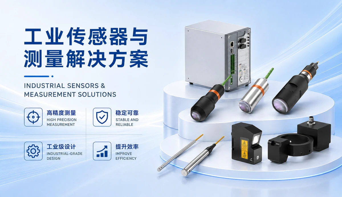
From a One-Sided Height Map to Warpage Decisions: A Silicon Wafer Scanning Method
This method uses an ST-P laser displacement sensor and a motion stage to build a one-sided silicon-wafer height map while controlling optical return, stage reference, scan coordinates, and evaluation rules separately. It also explains why that map is useful for process monitoring but is not automatically equivalent to free-state bow or warp under SEMI MF1390.
View detailsFAQ
Insufficient Wafer Warpage Accuracy: A Four-Layer Error Budget
When wafer scans correlate poorly with an accepted tool or reload variation is too large, allocate error across mechanics, optics, environment, and algorithms before selecting a finer sensor. Independent tests quantify stage straightness, specular return, thermal drift, support, and datum residuals so the corrective action targets the dominant contribution.
View details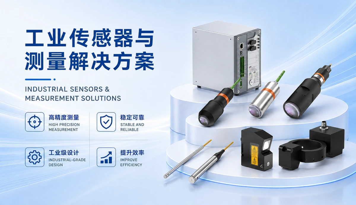
Application Notes
ST-P Series Laser Displacement Sensor for Semiconductor Package Chip Height Detection
This article introduces the application of ST-P series laser displacement sensors in semiconductor package chip height detection, including measurement principles, selection guidance, installation and commissioning tips, and common FAQs to help engineers achieve high-precision non-contact measurement.
View details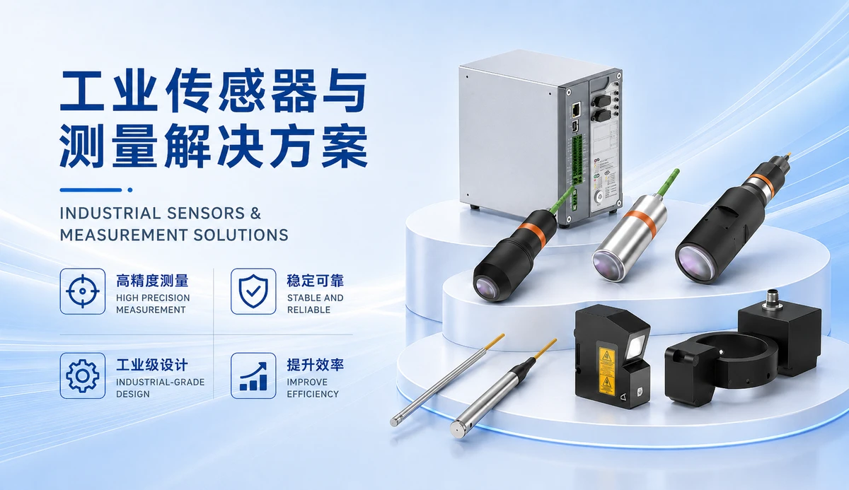
Application Notes
ST-P Series Laser Displacement Sensors for PCB/Substrate Component Height Measurement
This article introduces the application of ST-P series laser displacement sensors in PCB/substrate component height measurement, covering measurement objects, principles, selection recommendations, installation, and common issues, providing a reference for semiconductor automation inspection.
View details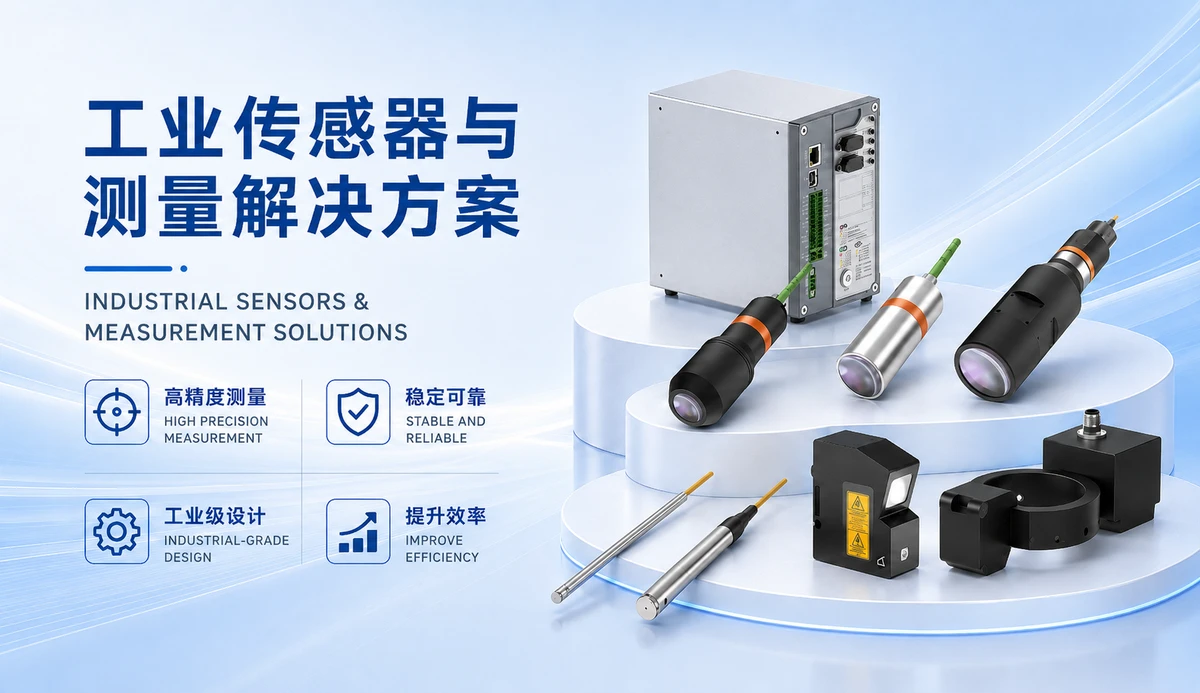
Application Notes
ST-P Series Laser Displacement Sensors in IC Substrate Step Height and Flatness Measurement
This article introduces the application of ST-P series laser displacement sensors in IC substrate step height and flatness measurement, covering measurement objects, on-site challenges, installation methods, selection recommendations, and precautions, providing a non-contact measurement solution for high-precision semiconductor inspection.
View details
Application Notes
Application of ST-P Series Laser Displacement Sensors in Wafer Dicing Height Difference Measurement
This article introduces the application of ST-P series laser displacement sensors in measuring height differences before and after wafer dicing, including detection objectives, on-site challenges, installation methods, measurement procedures, selection recommendations, and precautions, suitable for semiconductor manufacturing and packaging testing.
View detailsFeatured Products
Need an Industry Measurement Solution?
Share your application requirements and our sales or engineering team will follow up.