
Application Background
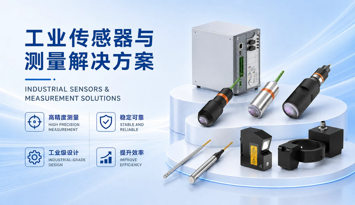
In semiconductor manufacturing, wafer handling robots are responsible for quickly and accurately transferring wafers between load ports, cassettes, or processing chambers. The height accuracy of the pick-and-place position directly affects whether the wafer is correctly placed or picked up. Excessive height deviation may cause wafer breakage, scratches, or equipment downtime. Traditional contact sensors have risks of wear and contamination, and are difficult to meet high-speed, high-precision requirements. ST-P series laser displacement sensors use laser triangulation non-contact measurement, providing real-time feedback on wafer surface height and precise position compensation signals for the robot.
Detection Object and Purpose
Detection Object: Wafer surface (silicon, gallium arsenide, etc.), wafer stage, vacuum chuck, gripper position.
Detection Purpose: Measure height deviation during wafer pick-and-place, wafer flatness, warpage, and Z-axis position of the robot end-effector to ensure smooth and accurate wafer placement or pickup.
On-site Pain Points
High Precision Requirement: Wafer thickness is typically hundreds of micrometers, and pick-and-place height error must be controlled within micrometers, which ordinary sensors cannot achieve.
Non-contact Need: Avoid scratches or contamination caused by contact sensors.
High-speed Response: Robot cycle time is fast; sensors need high-speed sampling capability for real-time position feedback.
Multi-material Adaptability: Wafer surfaces may be mirror-like, rough, or coated; sensors must adapt to different reflective properties.
Product Principle and Selection Guide
The ST-P series laser displacement sensor is based on the principle of laser triangulation. A laser beam illuminates the surface being measured, and the reflected light is imaged onto a CMOS/PSD through a lens. The displacement is obtained by calculating the change in the position of the laser spot. This series offers several models to choose from based on installation distance and accuracy requirements:
Model | Reference Distance | Measurement Range | Repeatability | Linearity Error
ST-P25: Reference distance 25mm, Measurement range ±1mm, Repeatability 0.05μm, Linearity error < ±0.6μm
ST-P30: Reference distance 30mm, Measurement range ±5mm, Repeatability 0.15μm, Linearity error < ±3μm
ST-P50: Reference distance 50mm, Measurement range ±10mm, Repeatability 0.25μm, Linearity error < ±4μm
ST-P80: Reference distance 80mm, Measurement range ±15mm, Repeatability 0.5μm, Linearity error < ±6μm
ST-P150: Reference distance 150mm, Measurement range ±40mm, Repeatability 1.2μm, Linearity error < ±16μm
For wafer height inspection, ST-P25 or ST-P30 are recommended due to their high repeatability and low linearity error. If installation space is limited or a larger measurement range is required, the ST-P50 or ST-P80 can be selected. Specific selection requires sample testing and verification based on the actual installation distance, wafer surface reflection characteristics, and on-site cycle time.
Solution Recommendations
Installation Method
The sensor can be fixed near the robot's base or end effector. The laser illuminates the wafer surface vertically or at a small angle. Bracket mounting is recommended to ensure the sensor is parallel to the measured surface and avoid angular errors. If measuring stage height, the sensor can be installed below or to the side of the stage, indirectly reflecting the wafer position by measuring the stage surface displacement.
Measurement Process
The robot moves to above the pick-and-place position.
The sensor emits a laser to measure the wafer surface height in real time.
The sensor sends the height data to the PLC or motion controller via Ethernet, RS485, or analog output.
The controller adjusts the robot's Z-axis position based on the feedback value to compensate for deviations.
The robot performs the pick-and-place action, and the sensor continuously monitors to ensure process stability.
Signal Output Method
The ST-P series supports multiple output interfaces:
Ethernet: Suitable for high-speed data acquisition and remote monitoring, directly connecting to host computers or industrial networks.
RS485: Ideal for long-distance transmission, connecting to PLCs or Modbus networks.
Analog (4-20mA or 0-10V): Compatible with traditional PLC analog input modules, offering high real-time performance.
IO Signals: Used for triggering or alarm, such as out-of-limit output.
In wafer handling scenarios, Ethernet or analog output is recommended to meet high-speed sampling and real-time control requirements.
Installation and Debugging Suggestions
Ambient Light Interference: Avoid strong light directly hitting the sensor receiver; add a light shield if necessary.
Vibration Effects: The sensor mounting base should be stable to avoid measurement errors caused by mechanical vibration.
Surface Characteristics: Wafer surfaces may be mirror-like, transparent, or coated. Adjust laser power or exposure time based on actual samples. It is recommended to conduct sample testing before formal application to verify measurement stability and repeatability.
Calibration: After installation, calibrate using a standard height block to ensure zero point accuracy.
Frequently Asked Questions
Q: Can the sensor detect transparent wafers?
A: Transparent materials (e.g., glass wafers) may cause laser penetration, leading to measurement deviation. It is recommended to use models optimized for transparent objects in the ST-P series, or adjust the installation angle to make the laser incident obliquely, reducing transmission effects. Performance should be confirmed based on the specific model.
Q: Will mirror wafers cause glare?
A: Mirror reflection may cause the spot to be too bright or saturated. Sensors with filters or automatic gain control can be used, or the laser incident angle can be adjusted to avoid perpendicular irradiation. Sample testing is recommended.
Q: Can the sensor sampling frequency meet high-speed robot requirements?
A: The ST-P series has a maximum sampling frequency of 160 kHz, which can meet most high-speed handling scenarios. Specific confirmation is needed based on robot cycle time and controller processing capability.
Conclusion
ST-P series laser displacement sensors, with high precision, non-contact measurement, and high-speed response, are suitable for wafer handling robot pick-and-place position detection. Through proper selection, installation, and debugging, the reliability and yield of wafer handling can be effectively improved. In practical applications, sample testing based on wafer material, surface condition, and on-site environment is necessary to ensure measurement performance. These sensors can also be extended to wafer flatness detection, warpage detection, package height detection, IC substrate step detection, probe station Z-axis position feedback, and other semiconductor high-precision inspection scenarios, providing strong support for semiconductor automation inspection.