
Application Background
In semiconductor packaging, chip height and coplanarity inspection are critical for package quality and subsequent soldering reliability. Traditional contact measurement risks scratching chips and suffers from low efficiency. The ST-P series laser displacement sensors, based on laser triangulation non-contact measurement, effectively address these issues and are suitable for wafer height measurement, wafer flatness measurement, wafer warpage measurement, package height measurement, and IC substrate step detection.
Product Principle and Selection Guide
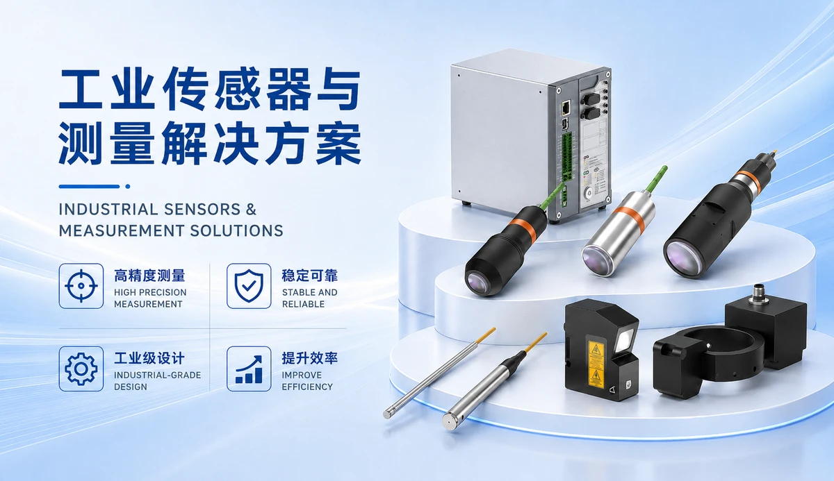
The ST-P series laser displacement sensors operate on the laser triangulation principle: a laser beam is projected onto the target surface, and the reflected light is received by a CMOS or PSD detector. The displacement is calculated from the position change of the light spot. The series offers multiple models to meet different measurement needs:
- ST-P25: Reference distance 25 mm, measurement range ±1 mm, repeatability 0.05 μm, linearity error < ±0.6 μm. Ideal for ultra-precision chip height measurement.
- ST-P30: Reference distance 30 mm, measurement range ±5 mm, repeatability 0.15 μm, linearity error < ±3 μm. Suitable for wafer stage height measurement.
- ST-P50: Reference distance 50 mm, measurement range ±10 mm, repeatability 0.25 μm, linearity error < ±4 μm. Suitable for package height measurement.
- ST-P80: Reference distance 80 mm, measurement range ±15 mm, repeatability 0.5 μm, linearity error < ±6 μm. Suitable for IC substrate step detection.
- ST-P150: Reference distance 150 mm, measurement range ±40 mm, repeatability 1.2 μm, linearity error < ±16 μm. Suitable for larger range height measurement.
When selecting a model, consider installation space, required accuracy, and measurement range. The maximum sampling frequency reaches 160 kHz. Output options include Ethernet, RS485, analog, and IO signals, enabling connection to PLCs, host computers, or motion control platforms.
Recommended Solution
For semiconductor package chip height detection, the following approach is recommended:
- Mount the ST-P sensor vertically above the chip surface on a wafer handling robot or probe station Z-axis.
- Set the sensor sampling frequency to match the production line cycle time (typically ≥10 kHz for high-speed lines).
- Transmit data in real time to a host computer via Ethernet or RS485 for height analysis and coplanarity judgment.
- For mirror-like metal or transparent encapsulation materials, perform sample testing to confirm stable reflection signals.
Installation and Commissioning Tips
Key installation considerations:
- Keep the sensor perpendicular to the target surface; tilt angle should be less than ±5°.
- Avoid direct ambient light on the sensor receiver; use a light shield if necessary.
- For highly reflective wafer surfaces, adjust laser power or use a diffuse target.
- Calibrate using standard height blocks to ensure linearity error is within tolerance.
Frequently Asked Questions
Q: Can the sensor detect transparent encapsulation materials?
A: Transparent materials may cause transmission or secondary reflections. Sample testing is recommended. Consider using a blue laser or adjusting the installation angle if needed.
Q: How to choose the sampling frequency?
A: Match the frequency to the line speed and motion velocity. For high-speed lines, use 160 kHz mode; for slower applications, lower frequencies can reduce cost.
Q: How to connect the sensor output to a PLC?
A: The sensor supports analog (4-20 mA or 0-10 V) and IO signals, as well as RS485 or Ethernet direct communication. Select the interface based on your PLC capabilities.
Summary
The ST-P series laser displacement sensors offer high precision, non-contact measurement, and high-speed sampling, making them advantageous for semiconductor package chip height detection. Actual applications require model selection based on specific conditions and sample testing for material characteristics. This article is for engineering reference only; specific parameters should be confirmed per model.